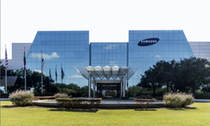
The world’s largest memory chip and smartphone maker is in discussions to locate a facility in Austin, Texas, capable of fabricating chips as advanced as 3 nanometers in the future, people familiar with the matter said. Plans are preliminary and subject to change but for now the aim is to kick off construction this year, install major equipment from 2022, then begin operations as early as 2023, they said. While the investment amount could fluctuate, Samsung’s plans would mean upwards of $10 billion to bankroll the project, one of the people said.
Samsung is taking advantage of a concerted U.S. government effort to counter China’s rising economic prowess and lure back home some of the advanced manufacturing that over the past decades has gravitated toward Asia. The hope is that such production bases in the U.S. will galvanize local businesses and support American industry and chip design. Intel Corp.’s troubles ramping up on technology and its potential reliance in the future on TSMC and Samsung for at least some of its chipmaking only underscored the extent to which Asian giants have forged ahead in recent years.
The envisioned plant will be its first in the U.S. to use extreme ultraviolet lithography, the standard for next-generation silicon, the people said, asking not to be identified talking about internal deliberations. Asked about plans for a U.S. facility, Samsung said in an email no decision has yet been made.


